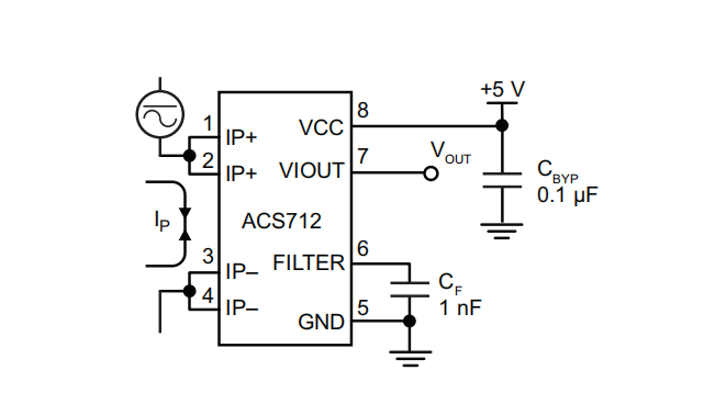
Allegro ACS712 provides economical and precise solutions for AC or DC current transduction in industrial, commercial and communication systems. The equipment package is easy for customers to implement. Typical applications include motor control, load detection and management, switching mode power supply, and overcurrent fault protection. The device is not suitable for automotive applications.
Typical Application

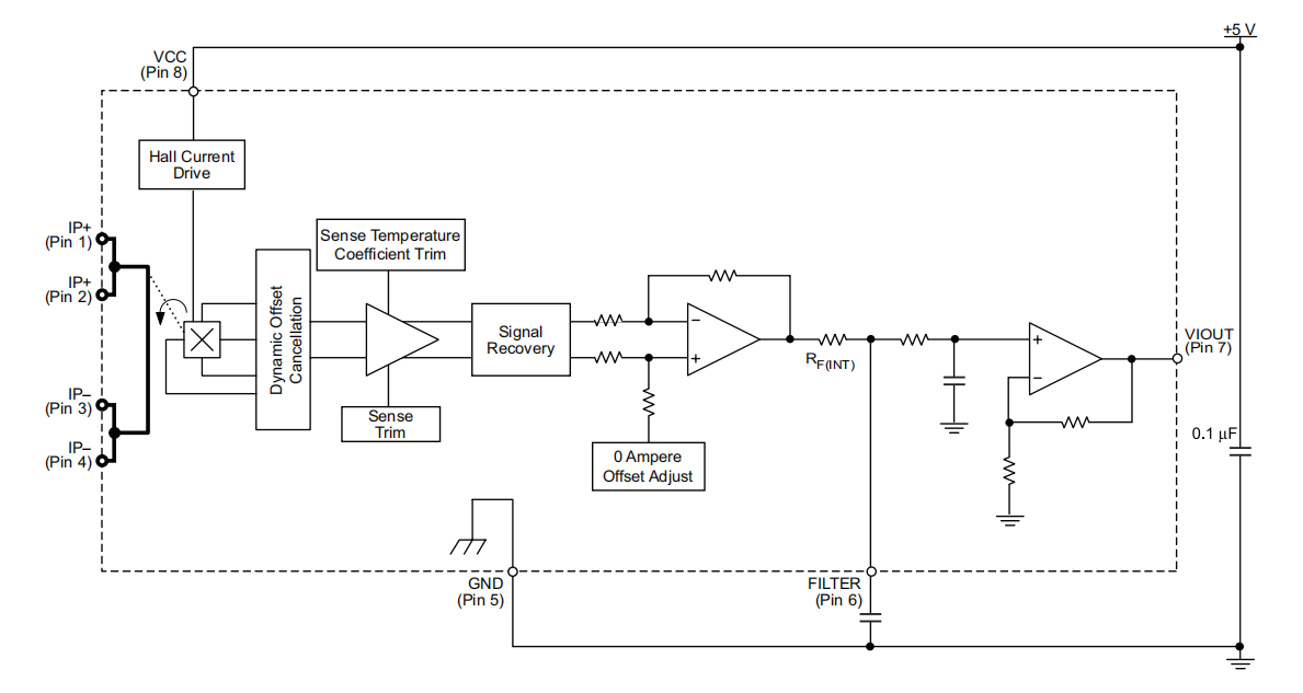
The device consists of a precise, low-offset, linear Hall circuit with a copper conduction path located near the die surface. Applying current through this copper conduction path creates a magnetic field, and Hall IC is converted into a proportional voltage. Device accuracy is optimized by the close proximity of the magnetic signal to the Hall transducer. Precise, proportional voltage is provided by the low-offset, cuter-stable BiCMOS Hall IC, which is programmed after packaging for accuracy. The output of the device has a positive slope. VIOUT(Q)), as the increased current flows through the main copper conduction path (from pins 1 and 2, to pins 3 and 4), this is the path used for current sampling.
Function block diagram

The internal resistance of this conductive path is typical of 1.2 mΩ, providing low power loss. The thickness of the copper conductor allows the device to survive up to five times the overcurrent conditions. The terminals of the conductive path are electrically isolated from the signal leads (pins 5 to 8). This allows the ACS712 to be used in applications that require electrical isolation without the use of optical isolators or other expensive isolation technologies.
The ACS712 is packaged in a small surface mount SOIC8 package. The lead frame is plated with 100% matte tin, which is compatible with the standard lead (Pb) printed circuit board assembly process. Internally, the device is lead-free, except for flip chip high temperature lead based solder balls, which are currently not subject to RoHS restrictions. The equipment is fully calibrated before leaving the factory.