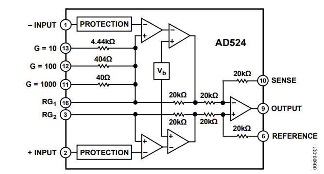
The AD524 is a precision monolithic instrumentation amplifier designed for data acquisition applications requiring high accuracy under the worst operating conditions. It adopts 16-pin ceramic DIP, 16-pin SBDIP, 16-pin SOIC wide package and 20-terminal lead-free chip carrier. The AD524's excellent combination of high linearity, high common-mode rejection, low bias voltage drift, and low noise makes it suitable for many data acquisition systems.
Functional block diagram

The AD524 has an output bias drift of less than 25 μV/°C, an input bias drift of less than 0.5 μV/°C, a CMR greater than 90 dB (120 dB at G = 1000) for ununit gain, and a maximum nonlinearity of 0.003% at G = 1. AD524 has a gain bandwidth product of 25 kHz (G = 1000). The output rotation rate is 5 V/μs, the settling time is 15 μs to 0.01%, and the gain is 1 to 100. It is suitable for high-speed data acquisition systems. As a complete amplifier, the AD524 does not require any external components to obtain fixed gains of 1,10,100 and 1000. For other gain Settings between 1 and 1000, only one resistor is required.
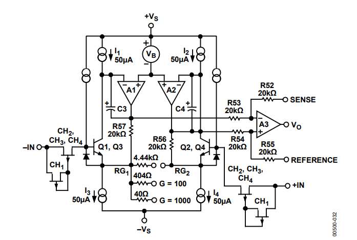
Test circuit

The AD524 input is fully protected in case of power-on and power-off failures. The AD524 is available in four versions for accuracy and operating temperature ranges. Economical Class A, low drift Class B, low drift, high linearity Class C is specified in the range −25°C to +85°C. The S-class is guaranteed to perform to specification in the extended temperature range from −55°C to +125°C.
Amplifier reduction circuit
